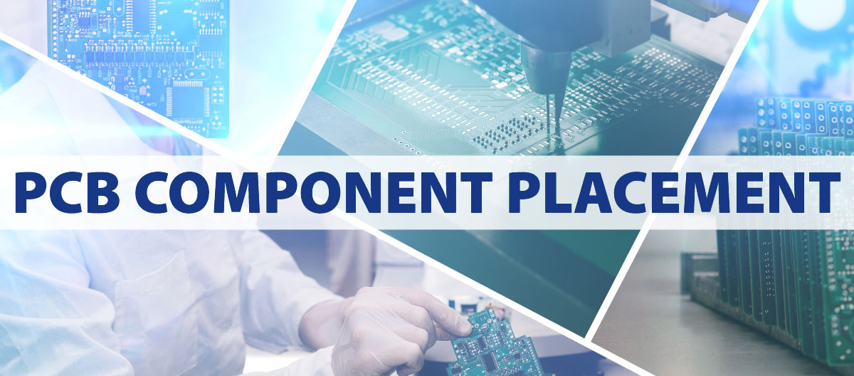
Why Component Placement Is Critical In PCB Assembly
Component Placement in PCB Assembly
Component placement – the process of precisely placing electrical components on a PCB assembly to create electrical interconnections between functional components and the interconnecting circuitry in the PCB – is a critical stage in the electronic manufacturing process.
Improper component placement can not only result in an aesthetically unpleasing PCB assembly, but it can also create a lot of problems in the future due to malfunctioning or defective products.
Here are some pro tips on proper component placement:
1. Understand Mechanical Constraints
When designing a PCB, it is important to consider the enclosure that the board needs to fit inside. Knowing exactly where mounting holes and edge connectors go is crucial for the size and shape of the board.
2. Consider Assembly Constraints
Before designing a board, consult with the manufacturer to understand how the board and components will be assembled and tested. The manufacturer should describe the assembly process, explaining the amount of space you have to work with on the board.
3. Don’t Place Integrated Circuits Too Close Together
AutoDesk suggests leaving at least 0.3500″ – 0.5000″ of spacing between each integrated circuit on a board and even more space for larger ICs. Placing ICs too close together can result in limited space when routing connection pins, wasting time rearranging the design.
4. Ensure Similar Components Are Oriented in the Same Direction
This makes the installation, inspection, and testing process simple for the manufacturer. Neglecting to orient similar components in the same direction can disrupt the soldering process and result in some parts not being soldered at all, which will leave the board with shorts and open circuits.
5. Minimize Connection Paths
For a simpler and more straightforward routing process, it is recommended to group parts to minimize intersections and crisscrossed connection parts.
6. Place Edge Components First
Placing edge components first will guide the board layout of input and output connections. These parts are typically components that cannot be moved due to a mechanical enclosure (e.g., connectors, switches, jacks, USB ports, etc.).
7. Do Not Overlap Parts
Overlapping parts can result in short circuits due to a stream of electricity crossing between components. Keep at least 40 mils of space between all parts.
8. Place All Parts on One Layer if Possible
Many designs require multi-layer PCBs to accommodate weight and space restrictions. However, if parts are placed on multiple layers, this can result in unnecessarily expensive manufacturing costs due to the need for a double pass-through in a pick-and-place machine.
9. Keep IC Pins and Polarized Components Aligned
Ensure ICs and polarized components are properly aligned to ensure no mistakes occur during the soldering and inspection process of the board.
10. Follow Schematic Design
Placing components in logical groups on a PCB layout like the schematic design will save time and minimize the length of traces since the parts have logically been grouped based on the schematic.
Quick & Precise Component Placement For PCB Assembly
Proficient in both automated and manual techniques for PCB assembly component placement, ThermOmegaTech® can meet the most rigorous and specialized design requirements for various industries.
With state-of-the-art automated machinery and a dedicated team of experienced professionals, we have the technology and expertise to process virtually any PCB assembly project with speed and quality.
ASM E-Place
ThermOmegaTech’s® ASM E-Place pick-and-place machine processes components down to 01005 and fine pitch down to 0.3mm (BGA, QFN, QFP).
Click here to learn more about our PCB Assembly capabilities.